|
||||||
My HF transceiver
Some basic theory
In the present time all the receivers with high characteristics implement the superheterodine principle. It means, that after optional preamplification input signal is transformed into fixed intermediate frequency by one or more steps. On this frequency, the main filtration and amplifications is done by different kind of band-pass filters and resonant amplifiers. The choice of IF is usually determined from availability of filters with desired characteristics. For communication receiver or transceiver the requirements for main selective element are very high, and usually two types of filters are used: electromechanical (f~200-500kHz) and quartz crystal (f~5-9 MHz). But if low IF is used, the relative difference in frequency between fundamental and mirror channels becomes to small for input signals with F>4-5 MHz, and necessary suppression of mirror channel becomes unachievable by using common resonant LC-band-filters.
That is why, all-band transceiver or receiver should have one of these things:
rather high fixed IF (for example 8.15 MHz) and appropriate crystal filter for it.
two fixed intermediate frequencies, the first one in range about 3-8 MHz, and the second one - about 465-500 kHz. In this case, main signal filtering occurs on the second IF.
variable first IF and fixed second IF. This is very common variant for homebrewed transceiver, because it has following very important advantage: variable frequency oscillator (VFO) works on rather low frequencies and is not switched by bandswitch. However, in this case all bands have the same width, which doesn't correspond with amateur radio frequencies
first IF higher, then highest received frequency, for example 35 MHz. This principle is used in many modern communication receivers. The advantage is, that no band-pass filters (BPF) are required for each band, because mirror frequencies are outside HF and can be suppressed by appropriate non-switchable low-pass filter at the input. But it requires high-frequency VFO (usually digital frequency synthesizer), which is difficult to make at home
My SSB/CW transceiver, that i describe below, has 2 fixed intermediate frequencies, the first one is 5.5 MHz, and the second (main) one is 500 kHz. This choice is not mine, i just followed the described UA1FA transceiver schematics. The main selective element is electromechanical filter with passing frequency range 500.3-503 KHz (bandwidth=2.7 KHz) , which perfectly fits for an SSB operation. For the CW operation the frequency range is additionally narrowed in the audio amplifier. CW-lovers may wish to add separate IF filter for this mode, though it seems to me unreasonable, at least for the beginner.
Most of amplification stages both in RX and TX channels use MOSFETs, because they have low noise, flat frequency response and ability to change gain remotely by changing the voltage on the second gate. The latter is used in AGC (automatic gain control) circuit and also in RX/TX switching to close unused channel. The only disadvantage of MOSFETs is rather high price (at least, in Russia) and ease to damage by static electricity.
Structure and blocks of transceiver
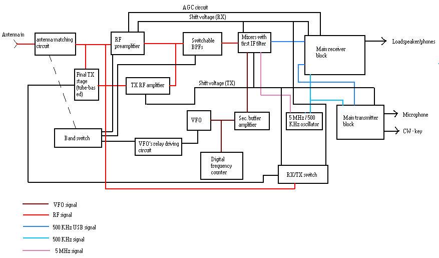
The described transceiver consist on following blocks:
Power supply, which gets -15V, +5V, +9V and +300V for various circuits.
Preselector and RF preamplifier, which uses dual-gate MOSFET and amplify the input signal before converting it into first IF.
Band-pass-filters for each band, they are switched by bandswitch by small-sized electromagnetic relays. Each filter consist on two resonant LC-circuits with connecting capacitors, which are chosen to provide flat frequency response within the band (there is no tuning of BPF occurring simultaneously with VFO tuning).
Mixers with first IF filter. There are 4 mixers (two in RX, two - in TX). All of them are identical and are made using JFETs. First IF filter has 3 identical resonant circuits with inductive connection. It is enough to suppress mirror-channel signals for 2-nd mixer.
Variable frequency oscillator (VFO) with internal buffer amplifier. The frequency of VFO is changed by variable capacitor and switched by bandswitch by electromagnetic relays.
External (second) buffer amplifier for VFO. It appeared to be required, because without it the influence of transceiver's circuit over VFO was too high, causing frequency deviation while transmitting and unavoidable 'jumps' o frequency by switching RX/TX (especially on high-frequency bands, 10 and 15m).
5 MHz/500 KHz oscillator, based on crystal stabilized generator with subsequent digital divider 1:10. 5 MHz signal is required for second mixer, and 500 KHz - for SSB/CW detector and SSB driver.
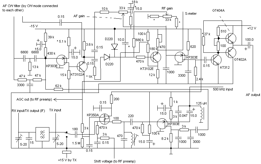
Main receiver block, consisting on electromechanical filter, dual-gate MOSFET IF amplifier, SSB detector, AF amplifier, AGC circuit and S-meter circuit.
Main transmitter block, consisting on SSB driver with microphone amplifier and CW generator.
TX power preamplifier with manual control of the gain.
TX power amplifier based on a tube (tetrode) with antenna matching circuit.
RX/TX switching block, which provides mode switching and supplies necessary control voltages onto second gates of some MOSFETs.
VFO's relay driving circuit. It reduces the driving voltage on the VFO's relay after switch, reducing also dissipating heat and decreasing frequency drift due to temperature change.
Digital frequency counter with multiplex display, which provides precise frequency measurement and indication
Everything else, like the case, variable resistors, S-meter, dynamical loudspeaker etc.
Here is structure diagram of the unit:
Power supply
This block, I suppose, is one of the simplest. The main problem is to find or to make i right power transformer, which gives ~45V AC at one output with middle point, 6.3V, 250V AC at other outputs with at least 40-50 W of general power. Avoid using small transformers, because during long operation they may overheat. The schematics of power supply is very common. Both -15 and +9V channels have the same design, the difference is only in zener-diode used and resistances of some resistors.
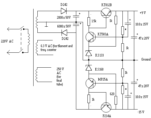
Resistors marked with a star (*) are chosen to provide necessary voltage at the outputs. Output transistors dissipate plenty of heat, so they should be adequate type and be placed onto well-ventilated radiator. Power diodes should be able to carry up to 1A of current.
I haven't placed here the schematics of 5 and 300V power supplies - they are very simple. 300V required for a final tube is obtained from a separate winding with diode bridge and 50 mF smoothing capacitor, and 5V required for digital frequency counter - from 6.3 V winding, which is used also for filament of the final tube.
RF preamplifier
RF preamlifier with preselector serves for initial filtration of input signal (improves dynamical range and mirror-channel selectivity) and its amplification. This stage, as well as many others, uses dual-gate MOSFET transistor as active element. Only such type of transistor provide high input impedance (required for high-Q preselector), low noise factor and possibility to change gain remotely in wide range (at least, 60dB).
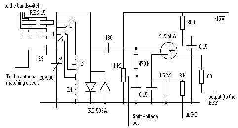
The input signal after passing through antenna - matching circuit, goes to the manual preselector, which consists on two coils and variable capacitor. Total inductivity in this resonant circuit is changed by bandswitch using small sized electromagnetic relays. I wouldn't recommend to provide the switching by some other way - wires, which form preselector must be as short as possible and shouldn't be closed to another circuits. Not obeying of this rule may lead to the instability of RF preamplifier, especially on high-frequency bands, and also to the decreasing of efficiency of preselector. Two diodes serve for the protection of MOSFET against possible strong signals. These diodes should be chosen carefully to avoid possible decreasing of preselector's Q and losses of signal. After the preselector, the signal goes to the first gate of transistor. A shift voltage about -12V is applied to the same gate. To simplify the circuit and to synchronize RX/TX switching in different blocks, the same voltage divider (semi-variable 1 Mom resistor) is used to provide shift voltage for another FETs in receiving channel. Through 3K resistor the second gate is driven by AGC circuit. 1 MOm resistor is used to protect the transistor while amplifier is disconnected from AGC (see MOSFET handling tips). Amplified signal goes though 100 Ohm resistor to the band-pass filters (BPF).
Coil L1 is wound on the plastic core 18 mm in diameter and has 3 turns of thick (1 mm) copper wire. It is the only coil used by working on 20, 15 and 10 m bands. L2 is wound on high-frequency ferrite toroid (20 mm outer diameter), it consist on 35 turns (sections starting from L1: 5, 12, 23 turns).
The BPF
The band-pass filters serve to attenuate undesired signals both by RX and TX. By receiving, they provide the mirror-channel selectivity together with antenna matching circuit and preselector (by chosen first IF mirror frequency is in 11 MHz away from fundamental one). On all bands BPF consist on two identical non-tunable resonant circuits coupled to each other inductively and capacitively. The connecting capacitors are chosen to provide flat frequency response within a band (very important especially on 80 and 10 m bands).
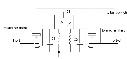
My attempts to follow the UA1FA schematics and using tunable BPFs failed - there were too many wires, and it yielded too much undesired couplings. Also, during long experiments i found, that the best way to provide good switching of BPFs is using relays. Unused filters are shorten to the ground to avoid undesired resonanses.
All coils in BPFs are wound on 6 mm polystyrene cylinders with a screwable ferrite slug. The distance between coils in each filter is about 25 mm. Number of turns for each band, as well as approximate capacities of C1-C3 are given in the table below.
|
|
|
|
|
|
|
|
|
|
|
|
|
|
|
|
|
|
|
|
|
|
|
|
|
|
|
|
|
|
|
|
|
|
|
Relays used in BPF may be the same, that in RF preamplifier. The only requirement for the implementation is compactness and short connecting wires. The latter is very important especially for 10 and 15 m bands, because there undesired acting of wires as additional inductors becomes very significant.
Mixers and first IF filter.
This block performs signal frequency conversion in two steps. By receiving, the input signal is converted into first IF (5.5 MHz) using VFO as local oscillator. After filtration, first IF signal is converted into second IF (500 KHz) using local quartz-stabilized oscillator. By transmitting, the order of frequency conversions is reversed, but oscillators and IF filter remain the same.
Each mixer is made using JFET and performs besides frequency conversion slight amplification of signal. The disadvantage of this design is that it is not balanced, or symmetrical, mixer. It means, that there are no suppression of LO signal at the output, and in case of transmission LO signal may go to the antenna and be transmitted. However, according to my experience, resonant circuits in this transceiver have together sufficient selectivity to avoid it. The advantage of this design is one - the simplicity and small number of components required.
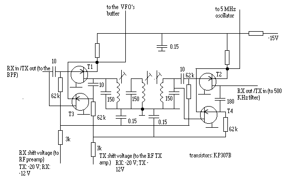
Working of this block:
In receive mode, transistors in TX channel (T3 and T4) are closed by high shift voltage (~20V) and do not work at all. RX channel transistors work under normal conditions required for JFETs, having ~ -12V on their gates. The input signal goes from BPF through 10 pF capacitor onto the gate of T1. To the same transistor VFO signal is applied. First IF signal is separated from the resulting mixture by the resonant filter, consisting on 3 identical LC-circuits. From the output of filter signal goes to the second mixer, which is similar to first one. Using 5 MHz signal, first IF is converted to the second IF, which is filtered in main receiver block by electromechanical filter.
In transmit mode transistors in RX channel (T1 and T2) are closed, and T3 and T4 work. 500 KHz USB (upper side band) signal from SSB driver or CW generator goes through 180 pF capacitor to the gate of T4. This transistor performs conversion 500 KHz USB -> 5.5 MHz USB. IF filter separates desired signal from the product mixture, and further conversion to the desired frequency is performed using VFO signal by T3. From the output of this block signal goes to BPF and further for TX power amplifier.
IF filter coils are wound inside 12 mm carbonyl iron cylinders with carbonyl slug. Each coil has 15 turns and resonates together with 150 pF at 5.5 MHz. The coils are mounted in the line, and distance between their centers is about 18 mm.
This block is not very critical for layout of components. The only requirement is compactness of IF filter (corresponding capacitors must beclosed to coils, and wires connecting mixers and BPF should be as short as possible (no more than 7-8 cm).
The VFO
This unit is very important one, because the absolute stability of frequency depends mainly on VFO (5 MHz/500 KHz oscillator is very stable due to using of quartz resonator). Therefore, extreme attention should be paid to the components, design and location of VFO in transceiver's case. Everything should be well fixed and soldered, especially components within oscillating stage. To reduce the influence of loading over the VFO, connection between oscillator and subsequent stages should be as weak as possible. This is very important in transceiver, because no frequency change greater than 100 Hz (max) is allowed by switching RX/TX. Also, if the VFO is affected some way by electromagnetic field of transmitter, another terrible effect may arise: frequency deviation. It means, that the frequency deviates from the setpoint in tact with your voice or key pressing. Such signal occupies wide bandwidth and is unreadable. It is sometimes very hard to avoid the frequency deviation, because high-frequency LO is affected by really everything. All precautions should be taken to place the VFO as far as possible from sources of RF radiation (final stage), as well as from sources of heat.
The VFO I am currently using is modernized UA1FA's design. It consists on oscillating stage made on high-quality bipolar transistor, 6 relay-switchable resonant circuits for each band, variable capacitor for master frequency control, a varicap, which provide splitting between RX and TX frequencies, buffer amplifier and additional voltage stabilizer.
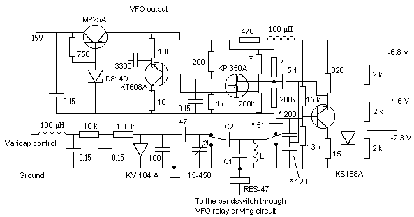
The oscillator is made by common-collector schematics on bipolar transistor. This transistor should have low p-n capacities (no more than 2-3 pF) and good frequency characteristics. The frequency being generated is determined by value of L, C1, C2 and several other capacitors. Actually, there are six L, C1 and C2 (for each HF band), and they are switched by six identical relays. Capacitors marked by star (*) can be changed to provide stable working and to reduce falling down the output voltage on 10 m band. All elements, which belongs to oscillator, must be temperature stable. Capacitors should be taken with TCC not more than 100x10-6 , material for inductor's cores should have also low temperature expansion coefficient.
From the oscillator, the signal goes through small connecting capacitor (5.1 pF) to the first gate of MOSFET. Shift voltages on both gates are controled by voltage dividers and should be set for maximum amplification and symmetrical signal cut-off. Emitter-repeater at the output gives to the signal necessary power and also serves as an additional buffer. But it appeared to be insufficient. That is why, additional buffer amplifier was introduced into schematics (see below).
The frequency of VFO is quite sensitive to the supplying voltage. That is why, all the VFO is connected to the main power supply through additional parametric stabilizer, which gives ~12V, and the oscillator itself and its varicap has also its own stabilizer (third (!) one, it gives 6. 8 V). 2.3, 4.6 and 6.8V outputs are used to control the varicap. By the transmitting, varicap is always fed by 4.6 V. If the ' RX/TX split' is on, the voltage on varicap may by between 2.3 and 6.8 V, providing frequency shift by RX.
The layout of components is extremely critical in VFO. All relays, coils and related capacitors should be mounted as close as possible to each other as well as to variable capacitor. Coils should be screened to avoid external influence. There shouldn't be any foreign wires near VFO's oscillator, everything should be properly fixed and placed. Avoid placing VFO near heat-dissipating elements, like final tube or power supply. The relays used should have a metallic case, which should be connected to the ground by soldering. It is good practice to place the entire VFO into hard screen, making all inlets and outlets through capacitors.
In my current variant, all coils are made on 6 mm screened plastic cylinders with adjustable ferrite slugs. Using the slug, exact frequency limit are set for each band. But it seems to, that it is not the best variant, especially for operation on 10-15 m due to rather low temperature stability. Anyhow, it is rather easy to make and good for beginning. The output voltage of VFO is about 3 V at 160 m band and decreases with the frequency down to ~1 V at 10 m. The frequency limits for each band are presented in the table below (actually, the bands are slightly broader, for ~30 kHZ from each side):
| Band | Lower limit, kHz | Upper limit, kHz |
|
|
|
|
|
|
|
|
|
|
|
|
|
|
|
|
|
|
|
|
|
|
|
|
Number of turns for each VFO coil depends on the construction. In my case it is about 20 turns for 160 m band and 8 turns for 10 m band. Capacity of C1 determines the frequency of VFO signal, and C2 - bandwidth. They should be chosen to provide necessary frequency limits for each band.
Second buffer amplifier for the VFO
It is done by the same schematics, that first one. I think, no additional comments are here required. 1k semi-variable resistor is used to attenuate VFO's signal before amplification and also to set the required signal amplitude for the mixer stage.
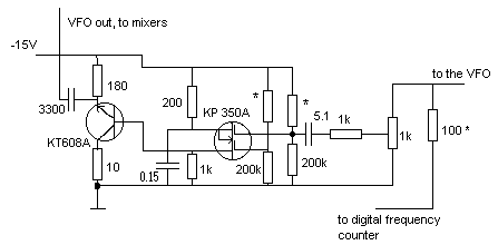
Resistors marked by the star (*) are chosen to provide maximum amplification and minimum distortion of the signal. Through 100 Ohm resistor the signal from VFO goes besides amplifier to the digital frequency counter.
5 MHz/ 500 KHz oscillator
In this block, two reference signals are produced from one quartz-stabilized generator at 5 MHz. Generator itself is made using JFET according to so-called three-point capacitive circuit. This generator has very high stability and is rather unaffected by loading. Therefore, only one emitter-repeater is used to drive mixers, compared to two buffer amplifiers required for VFO. Besides the output, 5 MHz sine signal is going to the half-wave former on diode and 1k resistor. The half-wave signal is gated to the input of digital divider K155IE2. This IC has two independent dividers inside: 1:5 and 1:2, the latter is just simple T-trigger. After passing 1:5 divider the frequency becomes 1 MHz and the shape of signal becomes short (0.2 microseconds) pulse. This signal is passing through internal T-trigger, becoming 500 KHz and symmetrical meander shape. This meander passes through the emitter-repeater and LC low-pass filter, which suppresses harmonics and makes the shape closed to the sine wave. All reset pins of IC are attached to -15V to provide correct functioning. The TTL IC requires +5V, so the ground pin is attached to -15V, and the power pin is grounded through appropriate resistor (ca 300 Ohm). This resistor should be chosen carefully to provide necessary voltage for divider IC.
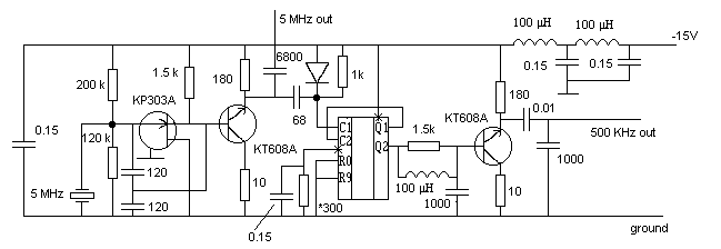
This block does not demand any precautions in the construction and is easy to make. The only adjustment required are setting the power voltage for IC and choosing minimal connecting capacitor, which still provide stable working of divider. In case of deviation of frequency from 5 MHz more than 100-200 Hz, additional serial inductors or capacitors to the resonator may be used.
This is the most complicated block according to the numbers of components, though i didn't have any problems with making and tuning of it. In this block occurs main filtration of signal in the electromechanical filter, amplification of resulting 500 KHz USB (upper-side band) signal, mixing it with 500 KHz signal resulting the audio frequencies, amplification of audio frequency signal up to ~100 mW for small dynamical loudspeaker. Besides loudspeaker, audio signal is going to the AGC amplifier, which drives the S-meter.
In the transmit mode nothing from this block is used except electromechanical filter, which is used in reversed direction compared to the RX. To avoid overloadings, the IF amplifier input is closed by the relay when TX mode is on.
From the second mixer the signal goes directly to the electromechanical filter. The trimmer on its input serve to provide a resonance on 500 KHz which improve the gain and frequency response of the system. After the filtration resulting USB signal goes to IF amplifier on the dual-gate MOSFET. The schematics of this stage is completely the same, that RF preamplifier. Shift voltage onto first gate is supplied through 3k resistor from RF preamplifier, and second gate is driven by AGC circuit. The presence os two stages (RF and IF) driven by AGC make the latter very effective, even on very strong signals. Resonant LC-circuit serves as a loading of IF stage, and from it amplified signal goes to the SSB/CW detector, which is made on the JFET. The schematics of the detector is almost the similar to the mixers, because the detector is actually the mixer, which produces AF signal at the output. The IF signal is applied to the gate of JFET through 200 pF capacitor, and 500 kHz signal - to the source trough two parallel capacitors. The AF is filtered by RC filter and then goes to the AF amplifier section.
Oh, it was a real pain to draw this picture.....
The AF sections starts from so called double RC- bridge band filter, consisting on three resistors and capacitors. It works only if wires indicated on the circuit rae connected to each other when CW mode is on. The result of it is that frequency response of the system becomes a peak about 600 kHz and therefore the bandwidth of whole receiver is narrowed. The first AF stage is made on JFET with subsequent emitter-repeater. Further, the signal goes two ways - to next stages and to AGC amplifier.
The AGC amplifier is made on KT3102E transistor, which has very high DC gain (about 700). AC signal is converted into DC by two diodes and charges the 10 microfarades capacitor. The voltage on the capacitor drives the transistor, which controls simultaneously S-meter and AGC circuit. When AF signal becomes larger, the positive voltage on the base (relative to the emitter) increases, which increase the drain current. The potential on 470 Ohm semi-variable resistor increases causing positive deviation of S-meter's arrow. Also, collector potential increases relative to the ground, causing increasing of the potential in the middle point of voltage divider 180k - 100k. This potential is applied to the second gates of two MOSFETs (one in IF amplifier, the second one in RF preamplifier), which yields in the gain decreasing. Also, the RF gain may be changed manually by a variable resistor. Two resistors marked by stars are chosen to provide proper work of the RF gain control: the right one is to provide necessary shift voltage on the base, when RF gain is on MAX ( right position of wiper on the circuit), and the left one is chosen to provide full opening of the transistor when RF gain is set to MIN. AGC circuit parameters are controlled by two values: resistance of resistor, which is in series to diode (I used 1 k) and capacitance of the capacitor. The first one controls the speed of charge of the capacitor, and the second one controls speed of discharge. These values are chosen to provide clear sound at the output of the receiver.
Besides AGC system, the AF signal goes to the final AF amplifier through the volume control potentiometer. The schematics of the latter is pretty common - JFET preamplifier, phase inverter and symmetrical output stage. Semi-variable resistor 100 Ohm is used to set the drain current in absence of signal to 10-20 mA, and another adjustable resistor (in my case - 27 k) is chosen to provide symmetrical cut-off os the signal. The overall gain of AF amplifier is quite high, and i had to introduce additional 10 k resistor in series to AF gain control.
Main transmitter block
Main transmitter block serves for the formation single-frequency CW signal at ~501 kHz or DSB signal at 500 kHz. It has microphone amplifier, balanced modulator, DSB signal amplifier and CW-generator.
In SSB mode, signal from microphone goes through 33 k potentiometer, which controls microphone gain, through low-pass RC filter to the microphone amplifier. This amplifier is quite sensitive, and it appeared to be required to make an additional voltage stabilizer for it, which gives -12V. Mike amplifier has three stages with the emitter-repeater at the end and it has very high sensitivity (less than 1 millivolt). To provide reasonable gain of the system as well as to avoid overloadings of modulator, 2k resistor is introduced after last stage. The only element to be chosen within the amplifier is the resistor in the base circuit of second stage. Its value should be set for maximal undistorted signal at the output. After the amplifier, AF signal goes to the passive balanced modulator on 4 diodes. This modulator is also fed by 500 kHz signal through semi-variable resistor, which is adjusted to the maximum suppression of bearing frequency. The output of modulator is loaded by primary winding of resonant transformer. The second winding forms a resonant circuit for 501 kHz, which drives the DSB amplifier on dual-gate MOSFET. The shift voltage on the fist gate is controlled by the voltage divider in TX RF amplifier block. In TX mode it is about - 12V, and in RX mode this stage is closed by applying -20V to the first gate. The potential on second gate is controlled by the internal voltage divider and determines the DSB gain of the system. From the output of DSB amplifier the signal goes through electromechanical filter, which is located in main receiver block. This filter cuts the low side band, forming an USB signal on 500 kHz, which then goes to the mixers block for further frequency conversion.
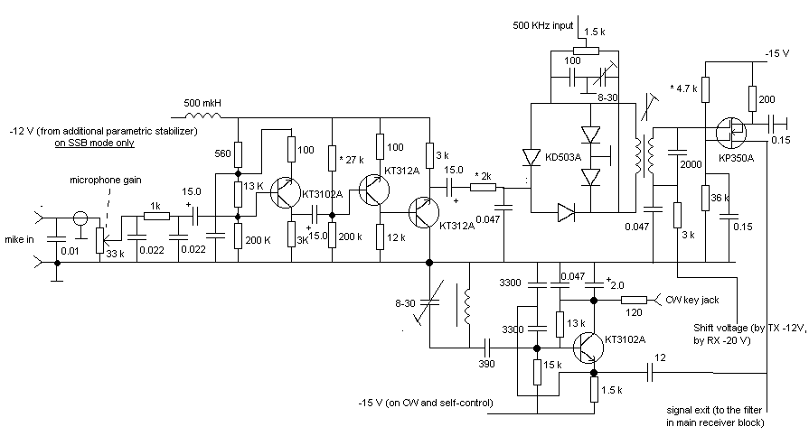
For operation on CW, and also for self-testing of the transmitter and tuning the antenna, this block includes CW generator, which produces the signal at ~501 kHz. This signal, as well as DSB goes to the filter through small capacitor (12 pF). The feeding of this unit is rather complex: DSB amplifier is fed constantly, microphone amplifier - only when SSB mode is on, and CW generator only when CW mode is on or by self control.
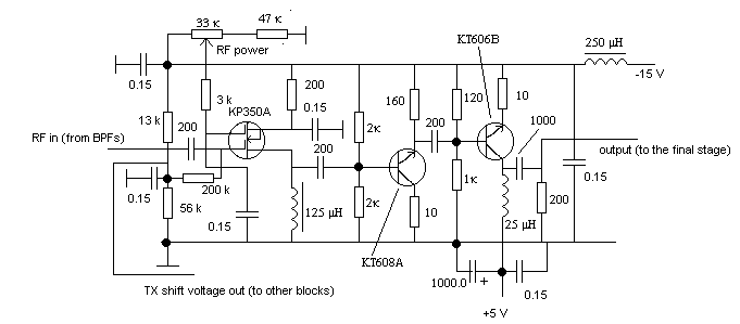
TX RF amplifier
In this block, formed HF signal after filtration by BPFs is amplified to 10 - 12 Volts for the feeding of the grid of output tube. The amplifier has 3 stages, the first one is a broad band stage on dual-gate MOSFET with inductive loading. The shift voltage on first gate of this transistor is controlled by the internal voltage divider. The same voltage is supplied to the TX mixers and DSB signal, which provides synchronous closing of TX stages, when RX is activated. The shift voltage on the second gate is controlled manually by the 'TX RF power' control. From the output inductor the amplified signal passes through emitter repeater on HF transistor and after it goes to the base of final transistor, which is fed by -15 and +5V. The total DC voltage on this transistor is about 20 V and it allows to obtain the undistorted signal up to 12 V in amplitude. This amplifier consumer plenty of power and in order to avoid cross-influences within transceiver is equipped by LC filters in the power line. From the loading resistor (200 Ohm) amplified signal with amplitude about 10-12 V goes to the grid of output tube. This block works quite stable, and usually nothing required to be adjusted. Since it uses high frequencies, input and output wires should be as short as possible and should have adequate positions to avoid interferences.
TX final stage
In contrast with many different blocks i described above, the schematics of this stage looks very simple. Yes, it does. But it is very critical to the design, because it operates with HF signals of big amplitude (up to 200 (!) V) and rather high power. The latter requires good and reliable screening of this stage from another. If there is some undesired inductive or capacitive connection, TX frequency deviation or total unstability of TX channel may result. Therefore, all components, including tube, inductors, two variable capacitors and the switcher must be placed in a metal box, which has proper contact with the case. Output stage generates plenty of heat, especially while transmitting. That is why, proper ventilation must be provided. I would recommend to install the cooler at the backside of the rig, like i did. This cooler sucks the air though holes on the top side of the case cooling all parts of the unit and providing stable working for long times.
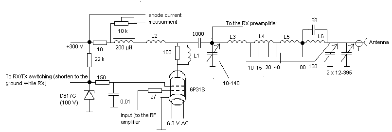
After transistor RF amplifier, the signal goes trough 27 Ohm resistor to the first grid of the tetrode. The potential on the second grid is stabilized by zener-diode and is about +100V. This provides anode current without a signal 45-50 mA and proper working of this stage in linear mode (By maximal signal anode current increases to 100-120 mA). In RX mode, zener-diode is shorten by the relay in RX/TX switching block. This causes full closing of this tube in receive mode. Anode circuit is fed by 300 V (Be careful!) through two inductors, which have very high impedance on HF. From anode circuit, amplified signal goes through 1000 pF capacitor to the antenna matching circuit, which consists on two variable capacitors and switchable inductors for each band. This is so-called P-network, which provides good filtration of harmonics (useful to prevent TVIs) and satisfactory matching with different antennas. From the same network signal is going to the RX preamplifier.
In order to control the anode current while working, I introduced the
possibility to measure it by controlling of voltage fall down on 10 Ohm
resistor by the same indicator, which serves as S- and P-meter. 10 k semi-variable
resistor is used to calibrate the meter.
Coils: L2 is wound on 10 mm plastic core and has 200 turns.
All the P-network coils are wound by thick (1 mm) wire on plastic cores.
They should be varied to provide proper working on all bands.
RX/TX switching block
This small block performs all necessary commutation by RX/TX switch. It has two identical relays, which works simultaneously. The following is switched:
In RX mode, -20V supply from a parametric stabilizer is connected to the 'Shift voltage' network of TX channel. This closes all stages, which are not needed by RX. In TX mode everything is reversed - -20V is connected to all RX stages.
In RX mode, 100 V zener diode is shorten to the ground, and in TX mode RX preamplifier's resonant circuit is shorten by the same way.
In TX mode, varicap in the VFO is permanently connected to the middle point of internal voltage divider (see VFO), but in RX it is connected to the 'RX/TX split' switch, which allows to offset the RX frequency.
Microampermeter in RX mode is connected to the main receiver block and works as an S-meter, but in TX it is connected to the detector of output signal through attenuator and serves to measure the level of output HF voltage, which is useful, for example, for antenna tuning.
Additional relay in main receiver block disconnects the IF amplifier from the filter while TX (see main receiver block).
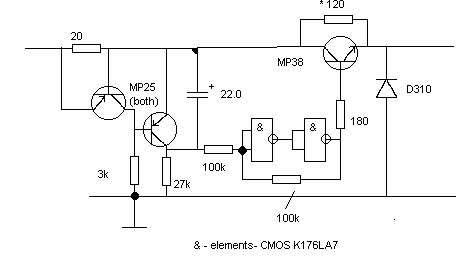
VFO's relay driving circuit
I think, this block is optional one. I introduced it in order to minimize the initial runout of frequency of VFO caused by the heat dissipated by VFO' relays. The principle of working of this circuit is following: When bands are switched by bandswitch, none of relays are connected to the block for a short time. During this time there is almost no current through 20 Ohm resistor and first pnp transistor is closed. In the same time second pnp transistor is open and electrolytic capacitor quickly discharges through it. This causes opening of npn switching transistor and supplying the full voltage to the relay. The relay turns on, and the first transistor opens, causing closing of the second one. Now, the electrolytic capacitor slowly charges through 27k resistor. When the voltage is enough to change the trigger state, T3 closes too and then relay is fed by reduced voltage, controlled by 120 Ohm resistor. The supplying volatge and resistor should be chosen according to relays parameters.
Digital frequency counter
I am not going to describe it here, because it is too difficult, especially drawing the circuit. This unit is made on 155 series (SN74) chips. There is really nothing special, just a quartz reference oscillator (5 MHz), frequency dividers and counters. The measuring time is 0.02 sec, but the input signal is divided into 2. This yields the resolution 0.1 KHz, which is enough for practical working. The input stage is made on JFET with following common emitter stage on HF bipolar transistor. For indication, vacuum luminescence indicator is used, which works in multiplex mode.
It appeared to be required to introduce the counter on/off switch,
which controls the power of most block schematics. The reason is,
that on several frequencies counter causes strong interference for reception,
which i was unable to get rid of.
If you want to know more about this block, just
write me a letter, feel free.
To the end of the description, i would like to describe the controls of the rig. In my current variant i have the following:
Two variable capacitors, which belong to antenna matching circuit ( see TX final stage).
Variable capacitor of RX preselector (see RX preamplifier)
VFO's variable capacitor, which controls the frequency of transceiver
'RX offset' variable resistor, which change the voltage on varicap in the VFO in RX mode only
'RX offset' switch. If it is off, 'RX offset' resistor does not affect the frequency. If it is on, it does, but in TX the frequency remains unshifted. This helps to operate with splitted frequencies and to 'look around' your frequencies without touching the main control.
Four gain controls: AF and RF gain controls (see main receiver block), Microphone gain (see main transmitter block) and RF power control (see RF TX amplifier)
Mode control: SSB, CW and self-control. In self control mode everything is connected like CW, but the CW key is shorten ('pressed').
Meter switch: S-P / anode current. In S-P mode, the microampermeter is connected to the RX/TX switching block, and in 'anode current' - to the final TX stage.
Digital frequency counter on/off switch.
Loudspeaker/Phones switch, which directs the output signal to the internal loudspeaker or to the phones jack.
Mains switch.
Three jacks are mounted on the front panel: for phones, for microphone and combined jack for RX/TX switch and CW-key.
Antenna connector (BNC type) is mounted on the rear panel of the unit.
73!, Valentin Gvozdev , RU3AEP.
![]()
