Dipolar power supply with over-current and over-heating protection by RU3AEP
Dipolar power supply with over-current and over-heating protection by RU3AEP
Technical requirements for a power supply
The task of a common power supply is to convert the AC voltage, supplied to your apartment via electrical net, into DC with desired parameters. These parameters are: voltage, maximal current, residual pulsations, stability of the output voltage by changing the input one and internal impedance of the supply, which shows, how the voltage at the output is changed by the loading variation. Two first parameters are derived from the purpose of the supply. Universal devices must have variable output, and the wider is the range, the better is the supply. The less are residual pulsations, the more ideal is the supply. For high-quality devices, amplitude of pulsations must not exceed 0.1% from the DC component. Two last parameters show, how stable the output voltage is. If the internal impedance is rather high (say, several Ohms), by high loading the voltage drops down too much, causing terrible non-linear effects in the equipment, which is being fed. I think, 0.05 Ohm is OK for most common tasks - by such value, voltage drops down by 0.1V by the loading current 2 A. The device described here satisfies all the parameters listed above.
Types of power supplies
First of all, power supplies may be divided into 2 main types: linear and switching ones.
Linear supplies use a transformer, which reduces the line voltage to the desired value. Then, it is converted to DC, filtered, stabilized (optional) and goes to the output. Such devices are rather simple and cheap, but usually they have big 'power/size' ratio and sometimes poor efficiency, which yields high heat dissipation. Nevertheless, they are widely used, and have big advantage - output is free from impulse interference, which is very important for working with sensitive radio equipment.
Switching supplies are much more 'young', than their linear analogues. They do not contain large transformer, which works on industrial frequency. Instead of it, input AC is interrupted (modulated) by the signal with frequency of several tens kilohertz. Such 'modulated' AC has a wide spectrum, which makes possible to use transformers, rated for high frequencies. These transformers have much lower sizes, compared to the classical ones, by the same thoroughgoing power. After transformation and electrical decoupling from the power line, the signal is converted to DC and treated further to achieve desired output voltage. These supplies have plenty of advantages, and they become greater and greater value in modern equipment - for example, all PCs use them. Due to the absence of big and heavy transformer, and big filtering capacitors, they can have very compact sizes by the significant output power, and their efficiency can be made closed to 100%. But they are much more complicated, require special components, like high-voltage MOSFETs, and have much more noise at the output, compared to linear analogues.
Power dissipation in linear power supplies.
As it was noted above, one big disadvantage of linear supplies is their rather low efficiency, which yields high heat dissipation.
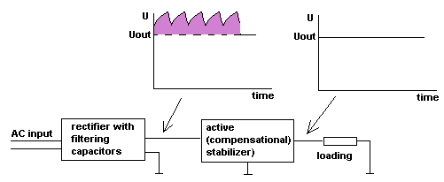
After the rectifier with the capacitive filter, the signal has quite significant pulsations, which increase with the loading and decrease with the increasing of capacitors. The stabilizer can work properly, if in any moment the signal at the input does not goes below output voltage (this is understandable - it can not provide 10 V at the output with only 8 volts at the input!). Practically, the performance of typical stabilizers degrades with the decreasing of input-output voltage difference, and a reasonable (3-4 volts) gap should be provided at the maximal consumed current. If the pulsations are significant, as they almost are in powerful units, the average input voltage has to be always at least by 5-6 volts higher, than the output one. This difference is 'cut off' on the stabilizer, causing dissipating of several watts per ampere consumed. I tried to represent statements above by the following diagram, where the area, which is responsible for the heat dissipation, is shown in pink colour.

In the supplies with variable output, the problem of heat dissipation becomes even more serious. If you decrease the output voltage, retaining the current consumed, the total power, consumed from the AC source, will not change at all. Its dissipation will just redistribute between the loading (useful dissipation) and the stabilizer (useless), causing increasing of the latter.
|
||||||||||||||||||||||||||||||||||||||||||||||||||||||||||||||||||||||||||||||||||||||||||||||||||||||||||||||||||||||||||||||||||||
Here is a table of dissipated power (in watts), which was calculated for the described power supply. U (input) is assumed 25 V (which is closed to reality), U (out) is varied from 3 to 20 V, and I (out) - from 0.5 to 5 A. As you see, the most heavy situation is by the combination of low output voltage and high current (110 watts is beyond all reasonable limits, so by the low output voltages the current should be limited to 2.5-3 A). 5 A by 20 V at the output cause the same power dissipation, as 1 A by 3 V. In general, this simple calculation shows a significant heat evolution by the stabilizers, so their controlling elements (transistors) should be chosen accordingly, mounted on the efficient heat sink with a low thermal resistance between the case and the sink. Even a good sink with a developed surface is sometimes unable to dissipate several tens watts of energy by keeping the temperature in safe limits. To increase the reliability and functionality of the unit, I introduced a cooler, which turns automatically when the temperature on the sink(s) rises above 50-60 oC
|
My construction |
General
The device I want to describe belongs to the class
of linear dipolar power supplies with compensational stabilizers and variable
output voltage. It has both over-current and over-heating protection systems.
The main characteristics are the following:
| Output voltage: | +3.5 - 20 V; -3.5 - -20V (variable) | |
| Maximal consumed current (from any channel): | approx. 5A (10-20V); 3A (3.5-10V) | |
| Residual pulsations (100 Hz): | less than 10 mV at 20V at the output and 3A of consumed current | |
| Differential internal impedance: | ~0.05 Ohm or even less | |
| Over-current protection system threshold: | 1 A - 7A (variable) | |
| Over heating protection type: | Automatic cooler control |
Actually, the unit consists on the following separate parts: a power transformer, diode bridge, filtering capacitors, main board, which contains stabilizers and over-current protection circuits, over-heating protection board and a number of commutation and indication devices, mounted on the front panel. Due to the dipolar output, there are 2 almost identical channels, one of which is responsible for the positive output, another one - for negative. These channels are almost independent - you may set the output voltage and protection threshold separately. If there is no need in dipolar feeding, but the voltage up to 40 V is required, two channels may be used simultaneously, without connecting to 'ground' point.
The only dependence between channels exists in protection circuit - if there is an overloading in one, another is turned off too (even if it is unconnected). This is done from safety precautions, because many schematics do not survive, if feeding of one polarity is suddenly turned off, but the second still remains.
The whole construction is reasonable to divide onto four parts, which are described separately:
Input circuits (transformer, rectifier, filter)
Main board of the unit
Over-heating protection board
Control and indication devices.
Input circuits
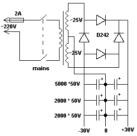
 The schematics of the input device is shown on the picture. There is really
nothing special and complicated, except the fact, that components used
have to be rated for the appropriate voltages and currents, which are rather
high. The power transformer should be rated for at least 200 Watts (40V
* 5A = 200 Watts), and from my experience the best ones have double-core
design. Such transformer have smaller sizes compared to classical ones,
and are much easier to disassemble and assemble, which is quite
important, if you wind the secondary winding by yourself.
I used a transformer, taken from old TV receiver. I removed all original secondary windings on it and wound one by myself, using 2 mm copper wire. The winding actually consists on 2 identical parts, each giving about 25 V of AC. It should be noted, that by such transformer and such wire diameter, the internal impedance becomes quite low, and currents in case of shorts are huge, may be several tens of amperes. In case of short, there will be diode and transistor burning, rapid transformer overheating and even melting of connecting wires. Therefore, any short should be avoided, and this supply definitely requires over-current protection.
After a transformer there is a diode bridge (diodes
are rated for 10A, not less) and filtering capacitors with overall capacity
9000 uF per channel. Since there are high currents, all interconnections
in these circuits have to be made from thick wires, and it would be great
to introduce a 10A fuse into every shoulder, but I haven't done it. At
the output, unloaded voltage is about 30 V in each channel.
Main board
Unfortunately, the whole schematics of the main board is too big to be represented on one picture (I receive the complaints sometimes, that some of my drawings are too wide and can not be printed correctly directly from the browser). As I said before, the supply has two identical channels, and therefore main board has two identical stabilizers and two identical over-current protection systems. The only difference between them is the polarity of the voltage - all p-n-p transistors in 'positive' channel are replaced by their n-p-n analogues in 'negative' channel.
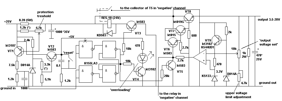
Let's see, how does this stuff works on the example of 'positive' channel. Its schematics is presented on the picture below:

The stabilizer itself
The compensational voltage stabilizer consists on transistors VT6-VT9, operational amplifier and associated circuits. It uses quite classical design: non-inverting input of the opamp is fed from the reference voltage supply. The inverting input is attached to the output of the unit through variable voltage-divider. The output of the opamp is connected to three-stage emitter-repeater, which acts as the current amplifier for the loading.
The principle is quite simple - due to the negative feedback loop, operational amplifier tries to keep the voltages on it's inputs equal. Even a small deviation from the equivalence causes serious voltage shift on the base of VT6 (due to very high DC amplification), which returns the system in the previous state. The feedback is rather fast (has very short delay time), and the system can easily 'follow' the pulsations, keeping the voltage at the output quite stable and providing very low internal impedance of the supply. Output voltage control is performed by the varying the division coefficient between the output and inverting input of the opamp. Since the inputs of the latter have equal potentials, the output voltage is determined by the following equation: U (out) = U (ref) * Kdiv. Because Kdiv can not be less than 1, the output voltage can not be less then reference.
The reference voltage supply is a two-stage parametrical stabilizer. The first stage is implemented on D814A, which gives about 12V with subsequent emitter-repeater on VT9. The second one is made on KS133 diode, which gives about 3.3V at the output. Such schematics has quite good parameters, since the stabilization coefficients of both stages are multiplied, and this provides quite clean and stable reference voltage even with a big pulsation on the input.
Over-current protection
The rest of the schematics is responsible for the turning the output off in the case if the output current exceeds some level (in this case, it is varied from 1 to 7 A by the corresponding potentiometer). There is a small resistor (0.39 Ohm), which is connected in series with the loading, and the voltage across it is proportional to the current consumed. As it may be seen, this voltage is applied between emitter and base of VT1, providing opening of the latter with the increasing of the current.
In case of overloading, VT1 opens and logical '1' appears on the lower (on the schematics) input of the trigger. The inverters on both inputs are required, because the driving level for the trigger is zero. The trigger changes its state, and this causes simultaneous opening of VT3, VT4 and VT5. VT4 is responsible for the LED control, which indicates the protection activity in case of overloading. VT3 controls the relay, which serves for 'closing' of another channel. The contacts of this relay connect the base of VT6 in 'negative' channel to the ground. Transistor VT5 is connected between the ground and the input of the current amplifier (VT6-VT8), and in the case of inactive state of protection system it is closed and does not have any influence over the working. By activating of the protection it opens and shorts the base of VT6 to the ground, causing decreasing of output voltage to zero. The protection works quite fast (several microseconds) and provides reliable protection of VT8 against burning. To reset the protection, a knob is pressed, which connect the second input of the trigger to the positive (+5V) internal source. This resets the trigger (and the entire system) into previous (inactive) state.
When you turn the supply on, there is some strong current, which charges the filtering capacitors on the main board. Since these currents are initially (some milliseconds) very strong, they will cause protection activating, and you will have to press 'reset' each time after you turns the unit on. To prevent this annoying event, a 0.1 mkF capacitor is introduced across the 'reset' knob. Its charging currents produce a high potential on the 'upper' trigger input, disabling the protection activating in first milliseconds after turning the unit on.
It should be noted, that a 'cross-connection' between channels exists, and the output may shut down also if the protection in another channel (negative one) is activated. In this case, corresponding relay shorts the base of VT6 to the ground.
Negative channel
As i said before, both channels are identical. All transistors in positive channel are replaced by their complementary analogues in negative channel (KT 3102 to KT3107, KT503 - to KT502, KT815 to KT814, KT819G - to KT818G). Diode's polarity is reversed. The only schematic difference is absence of two inverters before main trigger - there is no need in them. In general it is a good idea to keep the parameters of all components in both channels as closed to each other as possible, because this provides identical parameters and ease of the tuning.
I hope, that my explanations were clear to understand principles of the working and the order of tuning (what is responsible for what) of this schematics.
Over-heating protection board
As it was noticed before, the power dissipated o output transistors is quite big, especially in the case of combination of low output voltage and high consumed current. Therefore, these transistors should be cooled adequately to prevent overheating, because in the case of the latter, the full (30V) input voltage may go directly to the output, burning the schematics being fed. In this case, over-current protection system will be unable to help - it works only if output transistors are in order. Also, powerful output transistors are rather expensive devices, so I think, that their cooling is required, if you want to get a reliable unit.
The simplest method of cooling is mounting near the sinks a cooler, which will constantly suck the air and provide adequate ventilation. But it has one big disadvantage - the cooler works every time the unit is on, and it generates some annoying noise while working. Also, the cooler is not really required in many cases, if the supply gives some tens of milliamperes to the loading. So, I decided to build a simple system, which will continuously measure the temperature of output sinks and activate the cooler, if the temperature exceeds some predefined limit. After some attempts a simple schematics was created, which is not really a good thermostating device, but perfectly fits for its purposes.

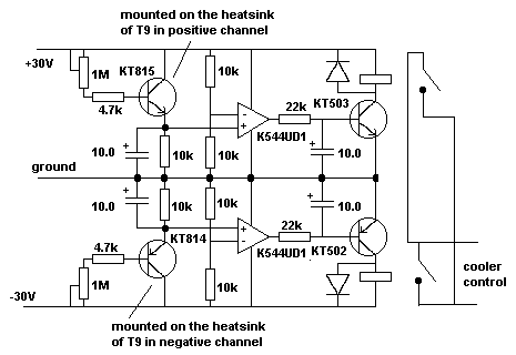
Here, two transistors, which are mounted on the corresponding heatsinks, serve as thermoelements. It is known, that if shift voltage is given to the base directly from the power supply through resistor, such stage is very unstable by temperature change, and it is not used in a good schematics. But if you want to make it thermo-sensetive, it is a good opportunity! As I measured, in the stages with presented design, the voltage on collector changes for several volts, if you heat the transistor from 20 to 60 oC - it is really a perfect and cheap 'thermometer', which is easy to integrate into electronic equipment. In positive channel, n-p-n transistor is used, in negative one - a p-n-p. Both protection channels are identical, except the structure of transistors and polarity of the diodes. The warmer the sink is, the larger is the voltage on the collector.
From the collector of 'measuring stage' the signal goes to the comparator, which compares it with the half of line voltage (~15V). The result of comparison determines the state of the key stage, which drives the cooler relay. Contacts of both relays are connected in parallel, so, the cooler is on if at least one heat sink is too hot. The only adjustable components are semi-variable resistors in base circuits of measuring stages. They should be chosen to provide cooler activating threshold at the temperature about 50-60 oC in both channels. Actually, the threshold temperature depends a little bit on the voltage in the line, and, therefore, on the loading of the supply and trends to increase with the increasing of the current consumed. But this effect does not play very significant role in the functioning of the protection system.
Control and indication devices
The unit has the following controls and indication devices:
Two variable resistors, which control the output voltage in both channels.
Two variable resistors, which control the protection threshold in both channels independently
Two LEDs, which serve as indicators of protection activating
The internal voltmeter with a limit 20V, which can be connected to any channel in order to measure appropriate output.
The internal ampermeter with a limit 5A, which can also measure current in any channel.
Two switches, one for the voltmeter, another one - for ampermeter. They choose the channel being measured.
Mains switch, of course.
I think, everything is clear here. As for meters, in my construction they were made from identical milliampermeters with a limit 10 mA by adding of appropriate resistors to them.
73!, Valentin Gvozdev
, RU3AEP.
gvozdev@mailexcite.com
| Глас народа |
|
02.11.2010 19:16 Да,чудиков у нас полноюКембридж наверное заканчивалю... -- and 24.08.2009 17:10 еще бы российскую версию.... -- 08.07.2006 17:06 Ну и для кого ты это всё написал? И выложил на Российском сайте. ... -- ur3fhv |